Multi-channel analog switch, multi-channel analog switch principle analysis
Author:Administrator Source:Site Views:630 Release time:2012/4/3 15:08:48
Multi-channel analog switch, multi-channel analog switch principle analysis
Integrated multiplexingAnalog switch(hereinafter referred to as multi-switch) is a commonly used device in important technical fields such as automatic data acquisition and program-controlled gain amplification, and its actual performance has an important impact on the rigor and reliability of the system. Regarding the application technology of multi-channel switches, there are two shortcomings introduced in some literature: first, there are more introductions to the device itself, and less introduction to the reasonable matching and coordination of the device and related circuits; Second, there are more introductions to principled things and less introduction to operational things. The results show that only by correctly selecting the types of multi-switch, paying attention to the reasonable matching and coordination of the multi-switch and related circuits, and ensuring that each circuit unit has a suitable working state, can the performance of the multi-switch be fully exerted, and even make up for the lack of a performance index and receive the expected effect. This article studies the application skills of multi-switch from the perspective of application. Multiswitches currently on the market toCMOSCircuits are the mainstay, so the following discussions, unless otherwise noted, are aimed at such products.
Â
1 Choice between "first break before on" and "first break before cut"
At present, most of the on-off switching methods of multi-switch on the market are "Break-Before-Make". In automatic data acquisition, a "first break and then on" multiswitch should be selected. Otherwise, the phenomenon of short connection of two channels will occur, and it will be damaged in severe cases
The signal source or the multiplexer itself. However, in program controlGain amplifierIn the case, if the feedback resistance of the integrated op amp is changed by using a multiplex switch to change the gain of the amplifier, it is not appropriate to use a "first off, then on" multiplexing switch. Otherwise, the amplifier will appear open-loop. The open-loop gain of the amplifier is extremely high, which can easily damage the normal operation of the circuit and even damage the components, and should generally be avoided.

2 Select the appropriate transmission signal input method
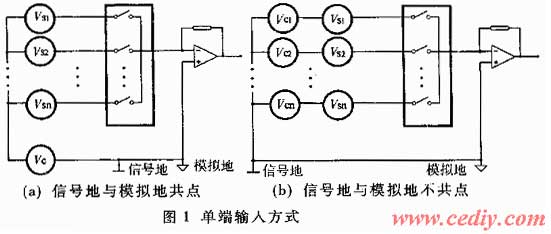
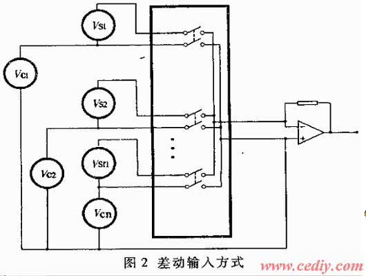
The transmission signal generally has two ways: single-ended input and differential input, which are suitable for different occasions. The single-ended input method is shown in Figure 1, that is, all signal sources are connected to the same signal ground at one end, the signal ground is connected to the analog ground of the ADC, etc., and the other end of each signal source is connected to multiple switches. In the figure, Vs is the transmission signal and Vc is the common-mode interference signal in the system. The advantage of the connection method in Figure 1(a) is that the number of channels does not need to be reduced by half, and the common-mode rejection capability of the system can be guaranteed; The disadvantage is that it only applies if all transmitted signals refer to a common potential and each source is exposed to the same noise environment, otherwise additional differential-mode interference will be introduced. The connection in Figure 1(b) applies to all measurements of the transmitted signal relative to the analog common ground of the system, and the signal level is significantly greater than the common-mode interference in the system. The advantage is that the maximum number of channels can be obtained, and the disadvantage is that the system basically loses the common-mode rejection capability. The differential input method is shown in Figure 2, which connects both ends of all signal sources to the inputs of the multiplex. The advantage is that it has strong resistance to common-mode interference, and the disadvantage is that the actual number of channels is only half that of the single-ended input method. When the signal-to-noise of the transmitted signal is relatively low, the differential input method must be used.
3 Reduce the effect of on-resistance
The on-resistance RON of the multi-channel switch (generally about 10Ω to 1kΩ) is much larger than the contact resistance of the mechanical switch (generally mΩ magnitude), which has a significant impact on the signal transmission accuracy of automatic data acquisition or the gain of the gain amplification of the process control, and the RON channel changes with the change of the power supply voltage, the amplitude of the transmitted signal, etc., so its influence is difficult to correct later. In practice, it is generally necessary to try to reduce the impact of RON to reduce its impact. Taking CD4051 as an example, the test found [1]: The RON of CD4051 varies with the change of supply voltage and input analog voltage. When VDD=5V and VEE=0V, RON = 280Ω, and it mutates with the change of V1. When VDD>10V and VEE=0V, RON = 100Ω, and it changes slowly with the change of V1. It can be seen that appropriately increasing the VDD of CD4051 is beneficial to reduce the influence of RON. It must be noted that while increasing VDD, the input logic levels of the strobe control terminals A, B, and C should be increased accordingly. For example, take VDD=12V (VEE=0V), you can use the power supply voltage pull-up clamp method, the resistance value of the pull-up resistor is more than 1.5kΩ, so that the effective high level of the gating control signal is not less than 6V. In this way, the CD4051 is ideally turned on (RON is small), and the conversion of CMOS level to TTL level (μP is generally TTL level) is realized.

It can be seen that according to the specific situation, appropriately increasing the power supply voltage of the multi-channel switch is an effective measure to reduce the impact of its RON. In addition, appropriately increasing the supply voltage can also reduce the on-resistance path difference ΔRON and speed up the switching speed.
4 Eliminate errors caused by jitter
Similar to mechanical switches, multiswitches also have jitter during channel switching, and transients occur. If the output signal of multiple switches is acquired at this time, a large error may be introduced. For example, [2]: A computer automatic data acquisition and processing system collects three analog quantities: pump speed, flow, and pressure. The TTL levels corresponding to the three analog quantities are: 1.5454V, 1.5698V, 2.9394V. The acquisition system continuously collected these three analog quantities from channels 1, 2 and 3 10 times, and the acquisition results were located between 1.8554~1.8603, 1.5625~1.5673, 1.62207~1.62695, of which the error of 1, 3 and channel was very large. It is found that this error is caused by the system collecting data before the on-off switching of the multi-switch is stabilized.
There are two common methods to eliminate jitter: one is to use a hardware circuit to achieve (hardware method), that is, to use an RC filter to remove jitter; The other is to solve it with a software delay method (software method). In systems with μP, the software approach is superior to the hardware approach. As in the above example, as long as a loop statement is added to the original QuickBASIC data acquisition program to delay appropriately, the acquisition result is between 1.5454~1.5478, 1.5698~1.5722, 2.9394~2.9418, the acquisition accuracy is significantly improved, and the acquisition result is normal.
5 Increase switching speed
The switching speed of the multiswitch is related to its own structure, operating conditions, and the condition of the external circuit. In practice, the following points should be noted:
The average propagation delay time tpd for all multiswitches decreases as VDD increases. Taking CD4051 as an example [3], when VDD=5V, tpd=720ns; When VDD=10V, tpd=320ns; When VDD=15V, tpd=240ns. It can be seen that appropriately increasing the power supply voltage of the multi-way switch can speed up its switching speed. The internal resistance of the signal source Rs of the transmitted signal has an important influence on the switching time of the multi-switch. The analysis shows that under other conditions being equal, the switching time is approximately proportional to Rs, that is, the smaller the Rs, the faster the switch action. Therefore, for signal sources with high internal resistance (as is the case with some sensors), it is advisable to use an impedance converter (such as a resistor follower) to reduce the impedance and then connect to the multi-switch. In addition, reducing Rs also reduces the error caused by the shutdown leakage current of the multiswitch. When the system requires a large number of signal channels, the two-level connection shown in Figure 3 should be used. In Figure 3, assuming that the system requires a total of 32 signal channels, these 32 channels are divided into 4 groups, each group is connected to 4 secondary switches, and the signal is output by the secondary switches. If the output capacitance of each switch is C0, the total output capacitance is from 32Co to about 12Co, the time constant of the circuit decreases, and the switching speed increases. In addition, this connection reduces the total shutdown leakage current of the multiswitch from 31Iz to approximately 10Iz (set the shutdown leakage current of each switch to Iz), thereby reducing the error caused by the shutdown leakage current. For the above two effects, the more channels the more significant the effect. Of course, this connection method requires a relatively large number of switches and relatively complex gating control, so it is mainly used in occasions with a large number of signal channels.

At present, the multi-channel switches on the market are mostly found in RCA, AD, SILICONIX, MOTOROLA, MAXIN and other companies' products, with a wide variety, and large differences in performance and price (see the relevant product data sheets of relevant companies for details). When selecting and using a multiplexer, the focus is to meet the system's requirements for signal transmission accuracy and transmission speed, and the following two points must be noted:
First, fully understand the characteristics of the multiswitch, otherwise unpredictable problems may occur. For example, a CMOS multiswitch is off when the power supply is cut off, while a junction FET multiswitch is on when the power supply is cut off. If this is not noticed, the chip may be damaged due to the power supply being switched on.
Second, only when the multi-channel switch is reasonably matched with the relevant circuit and coordinated work can it give full play to its performance and even make up for the lack of some performance. Otherwise, the one-sided pursuit of high performance of multiple switches and neglecting the matching and coordination with related circuits will not only cause waste of cost and performance indicators, but also often fail to receive the expected results.
In addition, limited by the type of chip or application, there are often redundant channels in practice. Since the internal circuitry of the multiswitch is interconnected, the extra channels may generate interference signals, which should be handled appropriately if necessary. Example [4]: When testing the CC4097 and CC4067 multiplexing, it is found that the inputs of all redundant channels must be grounded, otherwise interference signals will be generated.